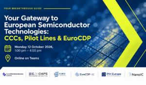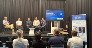


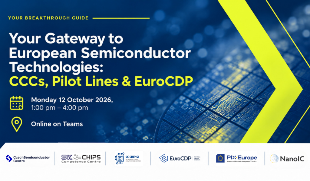
This joint webinar brings together three national semiconductor competence centres — KC ČIP.SI, Czech Semiconductor Centre and SK Chips — with key European semiconductor infrastructure: the European Chips Design Platform (EuroCDP) and the PIXEurope and NanoIC Pilot Lines.
Participants will gain a practical overview of the services available to companies, startups, SMEs, researchers and other innovators across Europe. The session will introduce opportunities in chip design, access to advanced technologies and pilot-line infrastructure, design tools, IP libraries and PDKs, as well as training and technical support. Speakers will also explain how users can access these services and how the competence centres can help them navigate the European semiconductor ecosystem and identify the most suitable support for their projects.
The webinar will conclude with an open discussion and Q&A, providing participants with an opportunity to discuss their needs directly with representatives of the competence centres, EuroCDP and the Pilot Lines.
This webinar is free of charge. Registration open tukaj.
Webinar Programme (13:00–16:00 CET)
13:00–13:05 | Welcome and Introduction (5 min)
Speaker: Petr Kamenický, Director of the CSC
Welcome, webinar objectives and introduction of the speakers.
13:05–13:15 | CSC Services at a Glance (10 min)
Speaker: Jana Drbohlavová, Deputy Director of the CSC
Role of the CSC, its main services and areas of expertise.
13:15–13:25 | SK Chips Services at a Glance (10 min)
Speaker: Martin Jagelka, Head of Partnerships
Role of SK Chips, its main services and areas of expertise.
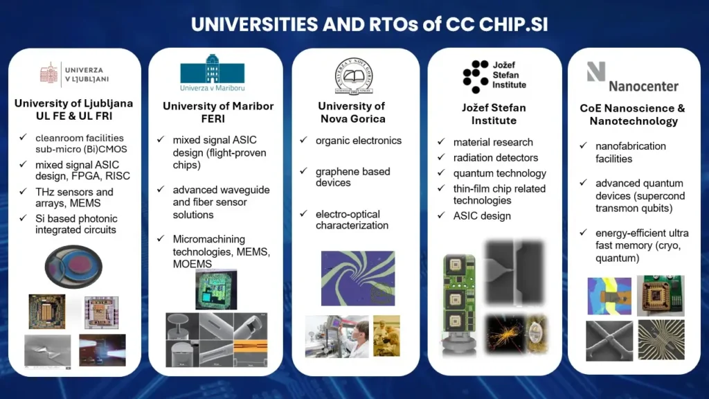
13:25–13:35 | CC Chip.si Services at a Glance (10 min)
Speaker: Jurij Podržaj
Role of CC Chip.si, its main services and areas of expertise.
13:35–14:05 | Introduction to PIXEurope (30 min)
Speaker: Marina Santana
Main technologies, available services, target users, access mechanisms and examples of potential applications.
14:05–14:35 | Introduction to NanoIC (30 min)
Speaker: Giuseppe Fiorentino
Main technologies, available services, target users, access mechanisms and examples of potential applications.
14:35–15:05 | Introduction to the European Chips Design Platform (EuroCDP) (30 min)
Speaker: Romano Hoofman
Design tools, IP libraries, process design kits (PDKs), training, technical support, and access to Pilot Lines, foundries, packaging and testing services.
15:05–16:00 | Open Discussion, Questions & Networking Session (55 min)
Moderated discussion with all speakers, questions from participants, exchange of experiences and networking opportunities.
16:00 | Closing Remarks
Speaker: CSC representative
Summary of key points, next steps and relevant contact information.
Additional information:
Trainings are organised upon request and tailored to the participant’s background and equipment availability.
Where:
on-line on Teams
When:
October 12, 1:00 pm – 4:00 pm
Contact:
For all information contact CC-Chip.si main office.
E-mail: office@cc-chip.si