

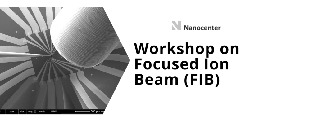
Online workshop on Focused Ion Beam (FIB)

About the training:

The participants will learn the basics of scanning electron microscopy (SEM) and FIB operations. They will learn about the FIB and SEM applications (cross-section analysis, analysis of defects on a chip, contact deposition, structure etching, 3D tomography, e-beam lithography, lamella fabrication…), and the limitations of the device. The workshop will be interactive, meaning the participants will be able to ask questions, and ask the operator to perform tasks they are most interested in.

What the training focuses on:

FIB capabilities

training is intended for:

Everyone interested in electron microscopy, especially SEM and FIB

Kje:

Online (Zoom link will be provided to participants)

Kdaj:

9 June 2026 at 9:00 AM (CEST)

Organizer:

Nanocenter

Kontakt:

E-mail: office@cc-chip.si

Rok za prijavo:

2 June 2026 (until 12:00 PM)

Applications are open and can be submitted via the form below.
INTERESTED?

APPLY HERE

OTHERS

MOGOČE VAS ZANIMA TUDI...

Lorem ipsum

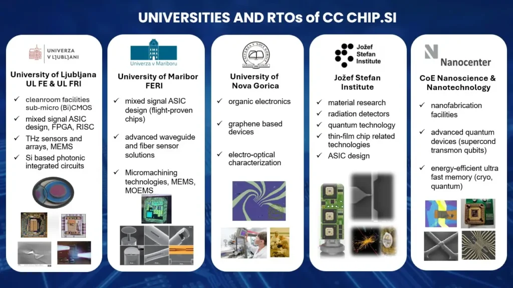
UNIVERSITIES AND RTOs of CC CHIP.SI

University of Ljubljana
UL FE & UL FRI
• cleanroom facilities sub-micron (Bi)CMOS
• mixed signal ASIC design, FPGA, RISC
• THz sensors and arrays, MEMS
• Si based photonic integrated circuits

University of Maribor
FERI
• mixed signal ASIC design (flight-proven chips)
• advanced waveguide and fiber sensor solutions
• micromachining technologies, MEMS, MOEMS


University of Nova Gorica
• organic electronics
• graphene based devices
• electro-optical characterization

Jožef Stefan Institute
• material research
• radiation detectors
• quantum technology
• thin-film chip related technologies
• ASIC design

CoE Nanoscience & Nanotechnology
Nanocenter
• nanofabrication facilities
• advanced quantum devices (supercond. transmon qubits)
• energy-efficient ultra fast memory (cryo, quantum)

Newsletter

Prejemajte tedenske novosti