TAKE ADVANTAGE OF

Infra-structure access

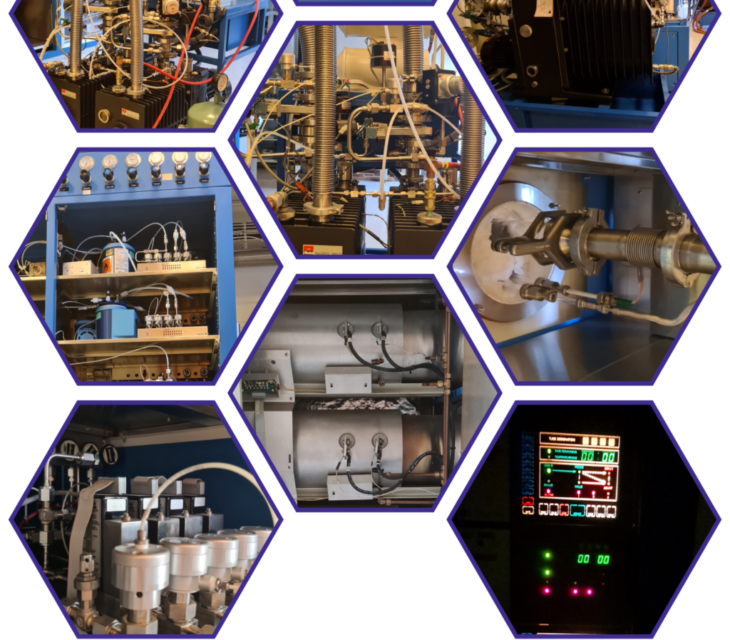
We provide you a list of available national equipment for semiconductor technologies – see below. Feel free to contact us for consultations on which equipment is most suitable for your measurements, proof of concept or innovation.

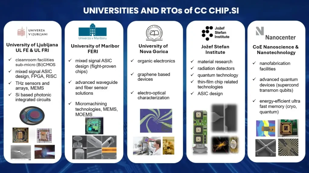
We assist you to use the EU infrastructure for chip design and fabrication. The centre provides access to pilot lines and virtual design platforms, supporting testing, development, and innovation in semiconductor technologies.

USE OF

National infrastructure

LET’S COOPERATE

Available equipment and infrastructure

Check the list of available national equipment.

LINK (COMING SOON!)

Consult with expert

Let us help you to select proper equipment for you

LINK (COMING SOON!)

Reserve equipment

We will help you with reservation.

LINK (COMING SOON!)

USE OF

International infrastructure

TAKE ADVANTAGE OF AVAILABLE EU PILOT LINES

FAMES

Flexible and Advanced MEMS & Electronics Services: flexible production of MEMS and microelectronics.

LINK

PIXEurope

Photonics Integration Europe: pilot line for photonic integration.

LINK

APCES

Advanced Packaging & Chiplet European Services: advanced packaging and chiplet integration.

LINK

NanoIC

Nanofabrication and IC prototyping: nanoscale fabrication and IC prototyping.

LINK

WBG

Wide Bandgap semiconductor pilot line: power electronics based on SiC and GaN.

LINK

DESIGN YOUR CHIP WITH EU DESIGN PLATFORM

EU design platform

Let us help you to access and use services of EU Design platform in designing your new chip.

LINK

AND

Other services

Lorem ipsum

UNIVERSITIES AND RTOs of CC CHIP.SI

University of Ljubljana
UL FE & UL FRI
• cleanroom facilities sub-micron (Bi)CMOS
• mixed signal ASIC design, FPGA, RISC
• THz sensors and arrays, MEMS
• Si based photonic integrated circuits

University of Maribor
FERI
• mixed signal ASIC design (flight-proven chips)
• advanced waveguide and fiber sensor solutions
• micromachining technologies, MEMS, MOEMS


University of Nova Gorica
• organic electronics
• graphene based devices
• electro-optical characterization

Jožef Stefan Institute
• material research
• radiation detectors
• quantum technology
• thin-film chip related technologies
• ASIC design

CoE Nanoscience & Nanotechnology
Nanocenter
• nanofabrication facilities
• advanced quantum devices (supercond. transmon qubits)
• energy-efficient ultra fast memory (cryo, quantum)

Lorem ipsum

Get weekly updates