

12. 10 – 23. 10. 2026
About the training:
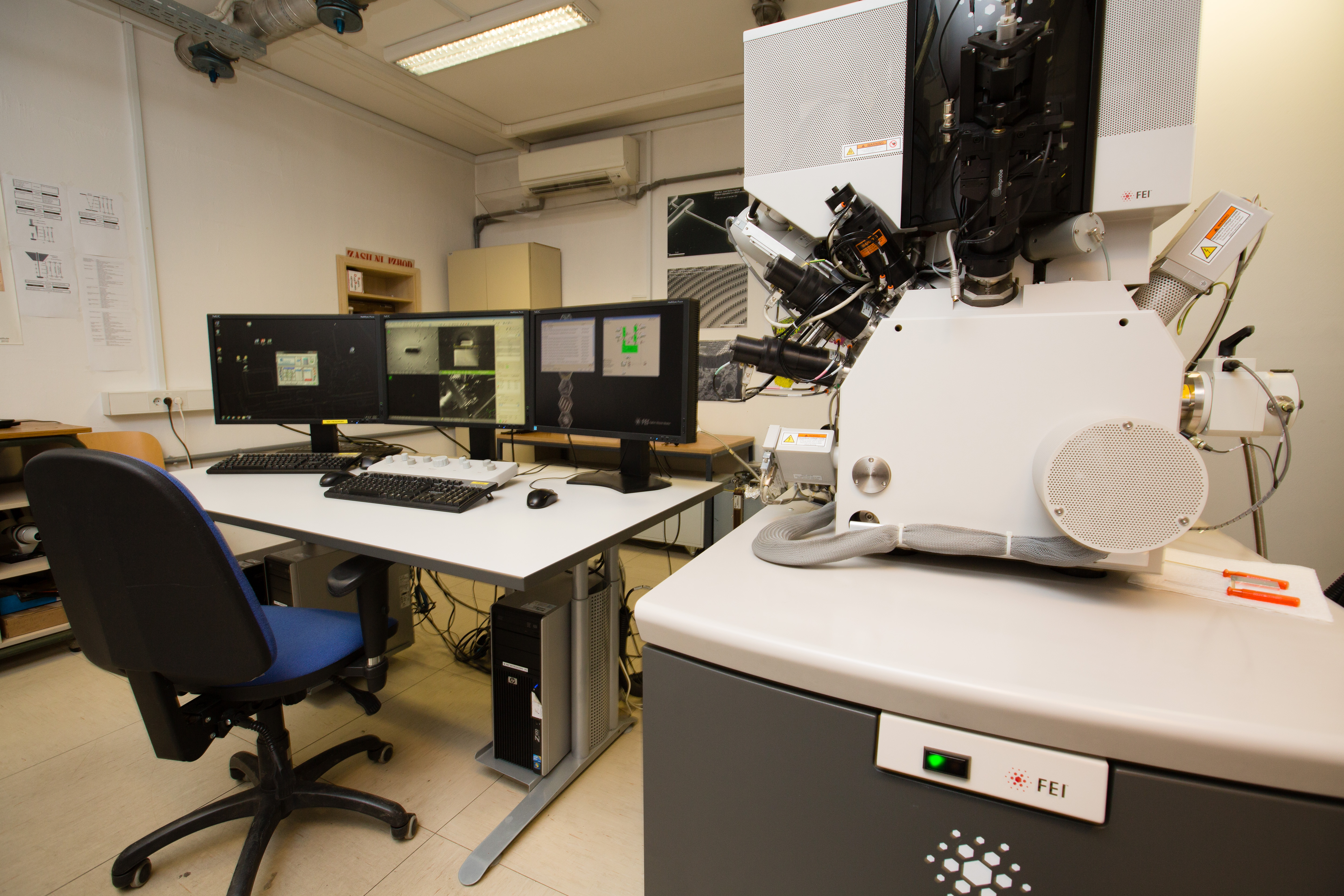
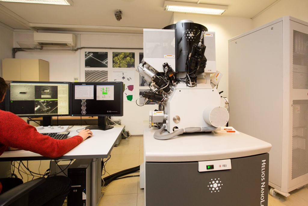
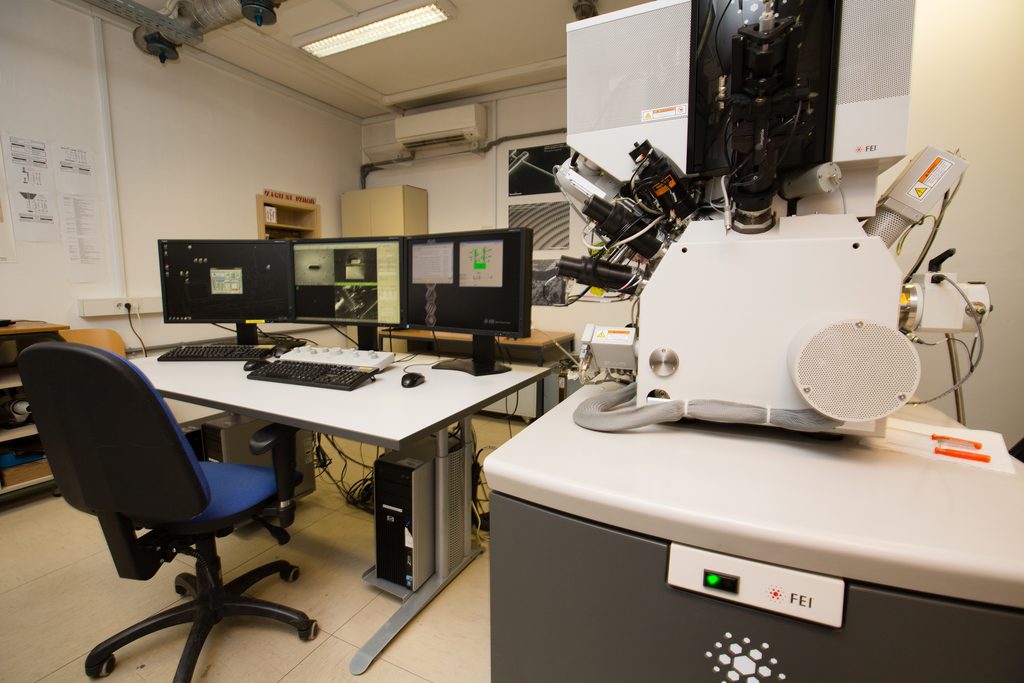
In the first step the trainees will learn the basics of scanning electron microscopy (SEM) and FIB operations. Then they will learn how to perform electron beam lithography using FIB with nanometre precision for the preparation of chips. They will also learn how to perform analysis of defects on chips with the cross-section technique. Defects will be thoroughly analysed using Energy-Dispersive X-Ray Spectroscopy (EDS) chemical analysis and with Scanning Transmission Electron Microscopy (STEM). For detailed 3-D analysis of samples on nanometre scale FIB tomography technique will be demonstrated. If there will be interest, also FIB lamella preparation training is also possible. The trainees will be able to use FIB during training under direct supervision of our instructors.
Who Should Attend?
The training is open to anyone interested in electron microscopy. Prior experience with electron microscopy and/or completion of a graduate- or PhD-level course in the field is recommended but not required.
Language:
Slovenian or English
When:
12. 10 at: 9:00 – 23. 10. 2026 till 12:00
Where:
Nanocenter, Jamova 39, 1000 Ljubljana, Slovenia
Topics:
- FIB/SEM
Overview of the Programme
Day 1 – FIB Fundamentals & Operation
- Introduction to FIB and FIB–SEM
- System components and functions
- Safety protocols
- FIB Pt deposition and chip fabrication
- Practical demonstration
Day 2 – Electron Beam Lithography & Defect Analysis
- EBL fundamentals and nanometer-scale patterning
- Practical EBL session using FIB–SEM
- Introduction to FIB cross-section techniques
- Hands-on defect analysis
Day 3 – EDS & Chemical Analysis
- EDS fundamentals and applications
- Practical FIB–SEM–EDS analysis
- Point spectra, line scans and elemental mapping
- Correlation of structural and chemical information
Day 4 – STEM Sample Preparation & Analysis
- Introduction to STEM
- FIB preparation of STEM/TEM lamellae
- Lift-out, thinning and final polishing
- STEM analysis and common imaging/analytical modes
Day 5 – FIB Tomography & Advanced Techniques
- Introduction to FIB tomography
- Slice-and-view 3D analysis
- Practical FIB tomography session
- FIB lamella preparation (optional/hands-on if time permits)
Learning Outcomes
Student will be able to become FIB operaters.
Additional Information:
Cost: Free of charge
Accreditation and Microcredential
Participants who successfully complete the course will receive a certificate of participation.
Organizer:
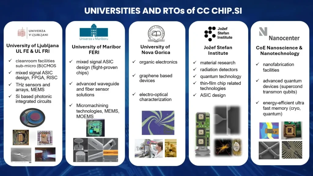
CC Chip.si and the Nanocenter Ljubljana
Registration:
Open until 5. October 2026
Contact:
E-mail: office@cc-chip.si