

About the training:
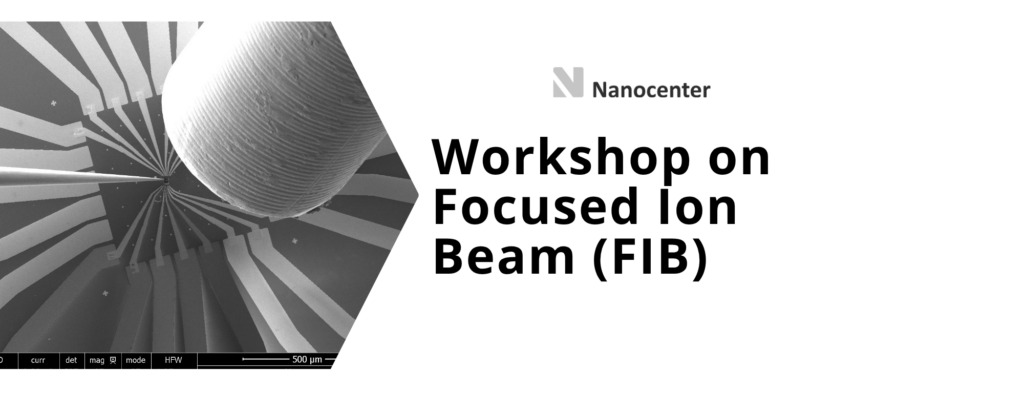
The participants will learn the basics of scanning electron microscopy (SEM) and FIB operations. They will learn about the FIB and SEM applications (cross-section analysis, analysis of defects on a chip, contact deposition, structure etching, 3D tomography, e-beam lithography, lamella fabrication…), and the limitations of the device. The workshop will be interactive, meaning the participants will be able to ask questions, and ask the operator to perform tasks they are most interested in.
What the training focuses on:
FIB capabilities
training is intended for:
Everyone interested in electron microscopy, especially SEM and FIB
Where:
Online (Zoom link will be provided to participants)
When:
6 Oct 2026 at 9:00 AM (CEST)
Organizer:
CC-Chip.si with Nanocenter
Contact:
E-mail: office@cc-chip.si
Application deadline:
1 Oct 2026
Applications are open and can be submitted via the form below.