

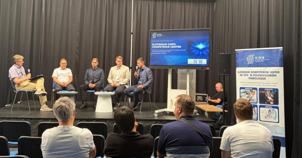
On 16 September 2026, as part of the International Trade and Business Fair (MOS) in Celje, CC Chip.si organised the round table “Chips and Semiconductor Technologies in Slovenia – Experiences, Opportunities and Challenges”. The event brought together representatives of L-TEK, Cosylab, SkyLabs, CC Chip.si and academia to discuss the current state, potential opportunities and key challenges facing Slovenia’s semiconductor sector. The discussion was moderated by Prof. Dr. Denis Đonlagić from the University of Maribor.
CC Chip.si and the Development of Slovenia’s Semiconductor Ecosystem
In the opening remarks, Prof. Dr. Janez Krč presented the primary objectives of the Programme for the Development of Chips and Semiconductor Technologies, highlighting CC Chip.si as one of the key measures already being actively implemented.
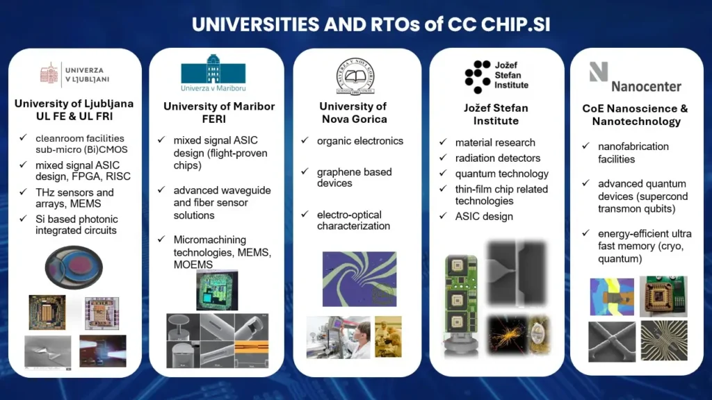
He presented the Competence Centre’s ongoing activities in specialised training, conferences, workshops, access to advanced technological equipment and consulting services. Among the educational initiatives, he highlighted the High-Level FPGA Design course, which awarded micro-credentials to participants. In addition, he presented ongoing efforts to map the technological equipment and infrastructure currently available across CC Chip.si partners, with the main goal of expanding this overview to the broader Slovenian semiconductor ecosystem.
Where Are Slovenia’s Key Opportunities?
The panel highlighted integrated circuit (IC) design and testing, application-specific chip design and niche applications (such as sensors and biomedical devices) as domains with significant potential for Slovenia. Participants emphasized that Slovenia cannot independently cover the full semiconductor value chain. Consequently, stronger collaboration among domestic stakeholders, deeper integration with European partners and a coherent strategic direction based on existing national expertise and industrial strengths are essential.
Talent and skills development were also a primary focal point. Industry representatives noted a persistent shortage of highly qualified professionals—particularly in circuit design and hardware development—stressing the necessity of providing students with hands-on industrial experience alongside rigorous academic training. Fostering closer ties between universities, research institutes and enterprises was identified as a critical priority.
From Design Tools to Prototyping and Infrastructure
The discussion highlighted several concrete bottlenecks hindering faster growth, including the high cost of Electronic Design Automation (EDA) software licenses and design tools, expensive fabrication and prototyping runs, and limited access to specialized infrastructure. Potential support mechanisms for SMEs regarding EDA tool access were discussed, along with the need for streamlined guidance on certification and market-entry requirements.
In this context, participants underscored CC Chip.si’s main role in connecting industry players with research organisations, delivering tailored training, and facilitating access to pilot lines, shared design platforms and technological infrastructure.
Looking Ahead
The round table concluded that advancing Slovenia’s semiconductor ecosystem will require sustained strategic focus, active industry–academia partnerships and continuous investment in specialized competencies. Building on existing expertise in chip design, niche applications and technological capabilities can provide a strong foundation for Slovenia’s future role in the European semiconductor ecosystem.