

About the training:
In this workshop, kids will fabricate an electrical switch made from graphene, known in electronics as a transistor. A transistor is the fundamental building block of electronic circuits. For example, at the heart of a modern computer, there are more than 50 billion transistors per square centimetre. In today’s electronics, transistors are primarily made from silicon.
About twenty years ago, researchers discovered that graphene could also be used to fabricate transistors—electrical switches that can operate much faster than their silicon counterparts. Graphene-based electronics is therefore the subject of extensive research at research institutions around the world.
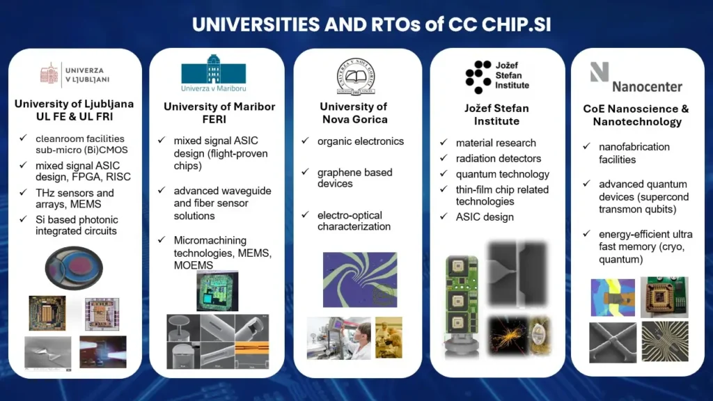
We also study graphene electronics at the Laboratory of Organic Matter Physics (LFOS) at the University of Nova Gorica (www-lfos.ung.si). One of the University’s missions in CC-chip.si is to transfer knowledge from research laboratories to society and, in doing so, encourage and inspire young talent.
During the workshop, participants will learn about a simplified process for fabricating a graphene transistor. The workshop will run for approximately six weeks, with one session per week, and will include:
- Producing graphene from graphite and observing graphene using an optical microscope.
- Designing the electrodes of a graphene transistor.
- Simulating transistor operation using dedicated software.
- Optical lithography of graphene transistor electrodes in the LFOS cleanroom (optional).
- Electrical characterization of the graphene transistor. In technical terms, this involves measuring its current–voltage (I–V) characteristics.
- Preparing a report documenting the entire process, from graphene preparation and transistor fabrication to the measurement and evaluation of the graphene transistor’s performance.
For who the training is intended:
talented primary-school and high-school kids.
Language: Slovenian
When:
- 7.9. 17h-19h Startlab Solkan
- 14.9. 17h-19h Startlab Solkan
- 18.9. 16h-18h LFOS Ajdovščina
- 21.9. 17h-19h Startlab Solkan
- 25.9. 17h-19h LFOS Ajdovščina
- 28.9. 17h-19h Startlab Solkan
- 5.10. 17h-19h Startlab Solkan
Approximate start and end time: 5 pm – 7 pm
Where:
- Startlab Solkan (https://startlab.si), address: Velika pot 33, 5250 Solkan, Slovenia
- LFOS – Laboratory of organic matter physics, University of Nova Gorica, Vipavska 11c, 5270 Ajdovščina
Topics:
Producing graphene from graphite and observing graphene using an optical microscope; Designing the electrodes of a graphene transistor; Simulating transistor operation using dedicated software; Optical lithography of graphene transistor electrodes in the LFOS cleanroom; Electrical characterization of the graphene transistor.
Overview of the programme
- 7.9. 17h-19h Startlab Solkan – Producing graphene from graphite and observing graphene using an optical microscope
- 14.9. 17h-19h Startlab Solkan – Designing the electrodes of a graphene transistor
- 18.9. 16h-18h LFOS Ajdovščina – Introduction to clean-room facilities
- 21.9. 17h-19h Startlab Solkan – Simulating transistor operation using dedicated software
- 25.9. 17h-19h LFOS Ajdovščina – Optical lithography of graphene transistor electrodes in the LFOS cleanroom
- 28.9. 17h-19h Startlab Solkan – Electrical characterization of the graphene transistor
- 5.10. 17h-19h Startlab Solkan – Final analysis and preparation of report
Learning Outcomes
- Explain the basic properties of graphene and its potential use in electronics.
- Prepare and identify graphene obtained from graphite using optical microscopy.
- Understand and design the basic structure of a graphene transistor and its electrodes.
- Simulate the operation of a graphene transistor using appropriate software.
- Fabricate and electrically characterize a graphene transistor, including measurement of its current–voltage characteristics.
- Analyse, document, and present experimental results and the complete transistor fabrication process.
Additional Information:
Cost: Free of charge
Organizer:
CC-Chip.si in collaboration with the University of Nova Gorica and StartLab
Registration:
There is a limited number of seats, registration is mandatory