High speed osciloscope
Osilloscope for measurement of fast electronic signals
RF Chamber
RF schielding chamber 2x3x3m light tight
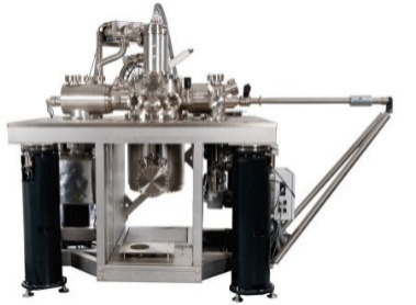
4-probe STM UHV system
The 4-probe STM UHV (LT Nanoprobe UHV System from Omicron Nanotechnology GmbH) system is a powerful microscopy system designed for characterization and pro…
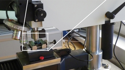
Revetest Scratch tester
The scratch tester is used for characterization of adhesion of thin films. It uses a diamond tip which is drawn along the sample surface by pressing a pred…
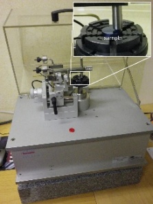
Tribometer 220V 50/60Hz
The tribometer is used for characterization of friction and wear. In its basic configuration it performs the standard pin-on-disk test where the disk is th…
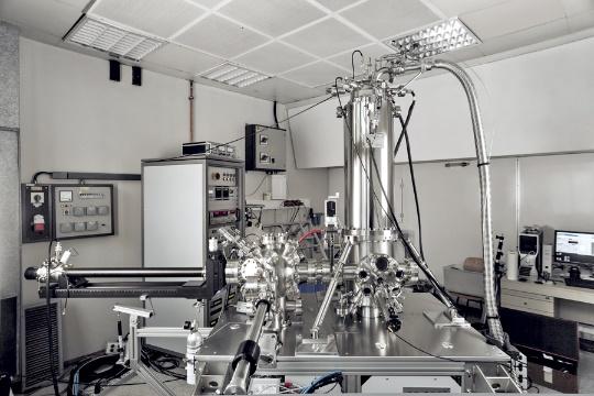
Low-temperature scanning tunneling microscope with supplements (LT STM)
This equipment allows (beside sample preparation) measurements with low-temperature STM at temperatures below 1K, which results in an exellent energy resol…
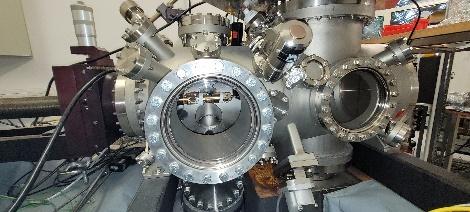
Nuclear magnetic resonance scanning tunneling microscope with supplements (NMR STM)
NMR-STM (Nuclear Magnetic Resonance–Scanning Tunneling Microscopy) is an extremely specialized STM variant that combines STM with nuclear spin resonance de…
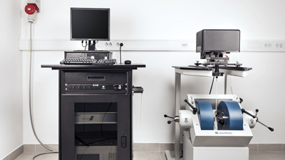
Vibrating Sample Magnetometer 7404 VSM
he magnetometer is used for basic characterizations of magnetic materials. The measured property is the dependency of the magnetic moment on the applied ma…
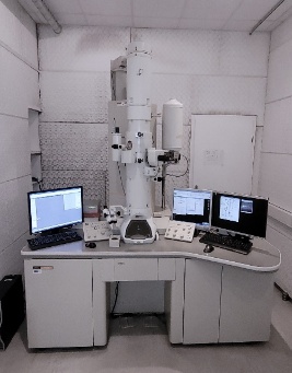
Transmission Electron Microscope (TEM) Jeol JEM 2100 HR
The JEM-2100 electron microscope provides solutions for a wide range of problems in the fields of materials, nanoelectronics, and biological sciences. Base…
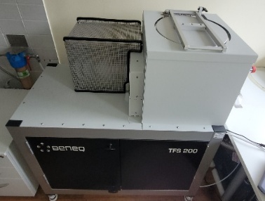
Atomic Layer Deposition – ALD System TFS 200
Atomic deposition system is intended for the application of different atomic layers. Since one of the goals in CENN Nanocenter is to test number of new nan…
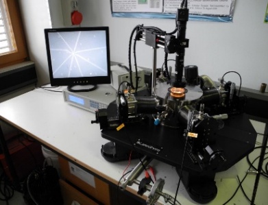
Low-temperature probe station TTPX Probe Station
4-probe probestation for measurements of electrical properties in temperature range 4K-400K. Each of the four probes can be moved in three degrees of freed…
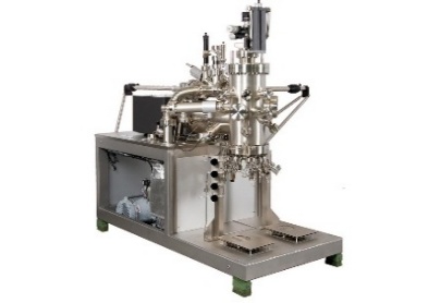
Molecular beam epitaxy (MBE) system
Molecular Beam Epitaxy (MBE) is a very precise deposition method for single crystal thin film growth. It can be used to deposit various materials, such as …
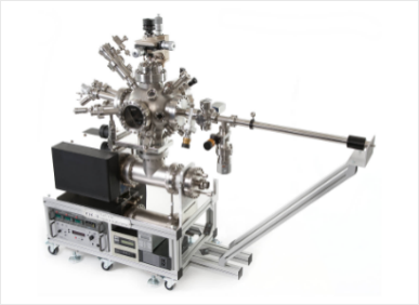
PLD (Pulsed Laser Deposition)
Pulse laser application is a technique for preparing thin layers of predominantly inorganic nature. The supplied system is intended for layer-by-layer grow…
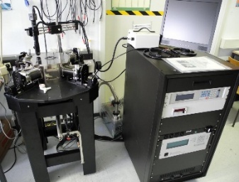
Low Temperature probestation with vertical magnetic field CPX-VF
4-probe probestation for measurements of electrical properties in temperature range 4K-400K and in a vertical magnetic field 0T – 2.6T. Each of the four pr…
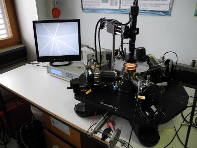
Low-temperature probe station TTPX Probe Station
4-probe probestation for measurements of electrical properties in temperature range 4K-400K. Each of the four probes can be moved in three degrees of freed…
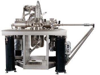
4-probe UHV STM/SEM microscopy system
The 4-probe STM UHV (LT Nanoprobe UHV System from Omicron Nanotechnology GmbH) system is a powerful microscopy system designed for characterization and pro…
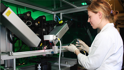
Elipsometer
Optical ellipsometry is a non-destructive technique for investigation of surfaces, interfaces and thin films. It probes modifications of the polarization s…
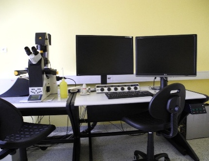
Confocal microscope LEICA TCS SP5 X
The equipment consists of a fully motorized inverted research fluorescence microscope with a confocal scanning head and one-photon excitation. Confocal mic…
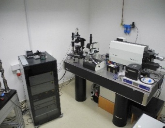
Confocal Raman spectrometer with AFM
TERS (Tip enhanced Raman spectroscopy) ready imaging Raman microscope – NT-MDT model »Integra Spectra for Material Science« provides »the same spot« couple…
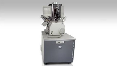
Focused Ion Beam Helios Nanolab 650
Focused Ion Beam (FIB) technique is a powerful micro- and nano-fabrication technique that uses a finely focused beam of ions—typically gallium—to image, mi…
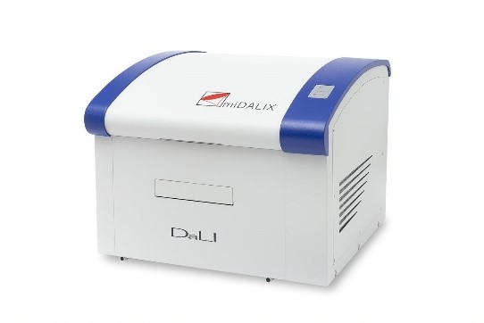
ProtoLaser LDI and Electron Beam Lithography – EBL
DaLI is a high resolution laser lithography system for rapid prototyping on resist-coated substrates. The platform is based on a continuous UV laser, 2D ac…
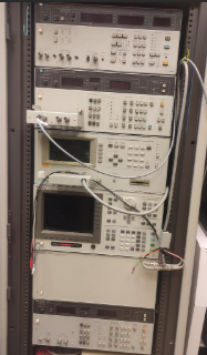
MicroWriter ML3 Baby Direct-Write Lithography System
The MicroWriter ML3 Baby is a compact, high-performance direct-write (maskless) optical lithography machine designed for rapid prototyping and small-volume…
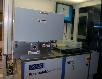
Plasmalab System 100 ICP180 – Deep Reactive Ion Etcher (Bosch process)
Advanced ICP-DRIE system for deep, high-aspect-ratio silicon etching using the Bosch process (SF6/C4F8). Capable of etching trenches and vias > 500 µm deep…
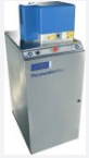
Plasmalab 80 Plus PECVD
Compact RF-PECVD system for deposition of high-quality SiOx, SiNₓ, SiOₓNᵧ and a-Si:H at low temperatures (50–350 °C). Electrode size up to 200 mm, excellen…
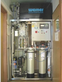
System for production of ultra pure deionized water (UPW)
Produces ASTM Type I ultrapure water (resistivity 18.2 MΩ·cm at 25 °C, TOC < 5 ppb). Continuous recirculation loop, 185/254 nm UV photo-oxidation, Duplex S…
HP 4155A Semiconductor Parametric Analyzer with Wentworth AWP 1050 Automatic Wafer Prober and associated instrumentation
Professional on-wafer semiconductor device characterization system for electrical measurements in a cleanroom environment. The core setup includes: HP 4155…
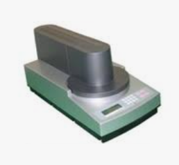
CMT-SR2000N Automatic 4-Point Resistivity Prober
Automated four-point probe system for precise sheet resistivity (Rₛ) and bulk resistivity measurements of thin films, wafers, and substrates up to 200 mm. …
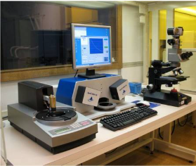
SpecEL-2000-VIS Spectroscopic Ellipsometer
The SpecEL-2000-VIS is a compact, bench-top spectroscopic ellipsometer designed for non-destructive thin-film characterization on semi-transparent flat sam…
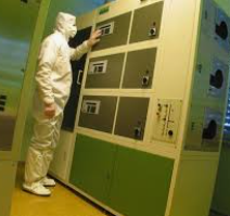
Tempress Omega Junior Diffusion Furnaces (3 stacks with 7 tubes)
The Tempress Omega Junior is a modular horizontal diffusion furnace system consisting of 3 independent stacks, each equipped with 7 process tubes for therm…
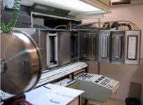
MRC 603 Sputtering System
The MRC 603 is a versatile RF magnetron sputtering system designed for thin-film deposition in cleanroom environments. It enables precise deposition of con…
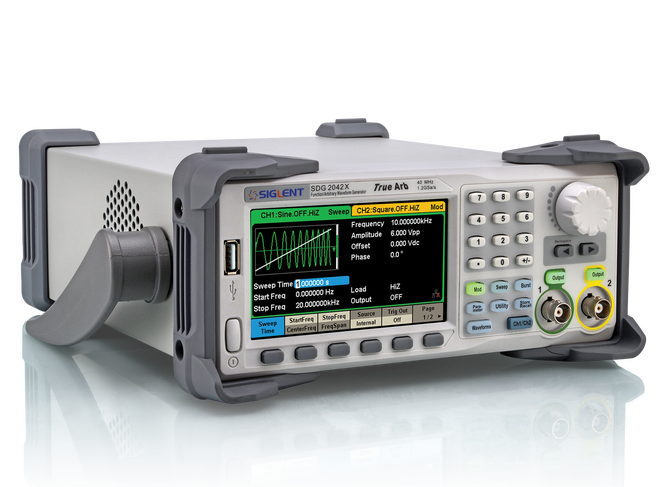
Arbitrary signal generator Siglent SDG 2082X
a dual-channel function/arbitrary waveform generator with a 80 MHz maximum bandwidth, 1.2 GSa/s sampling rate and 16-bit vertical resolution
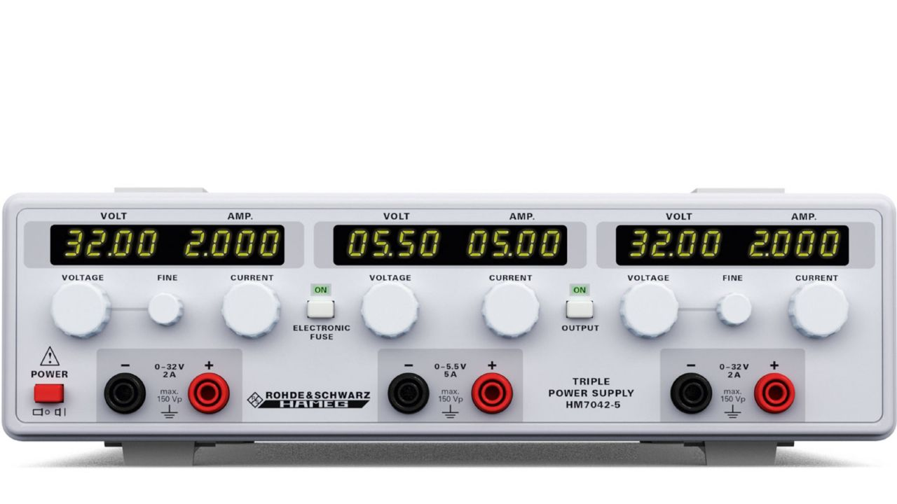
Tripple power supply HM 7042
2 x 0…32V/0…2A, 1 x 0…5.5V/0…5A
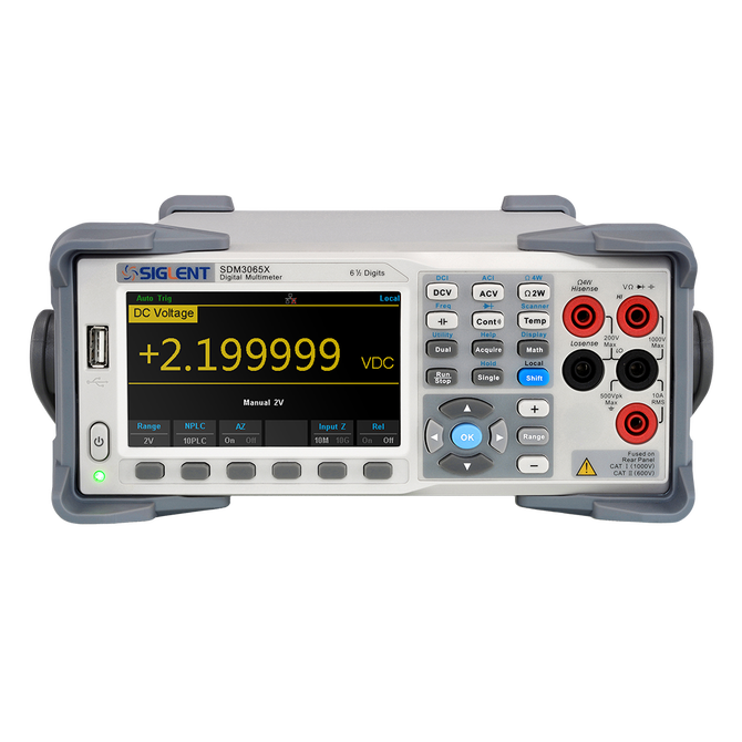
Digital multimeter Siglent SDM 3065X
a 6 ½ digit DMM with 12CH Scanner card (digital multimeter with 2,200,000 counts)
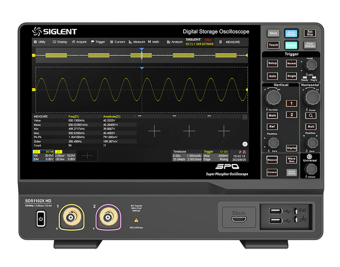
Osciloscope SDS 1102X
2 channel high resolution digital storage oscilloscope is based on 2 GSa/s, 12-bit Analog-Digital Converters and front ends with excellent noise floor perf…
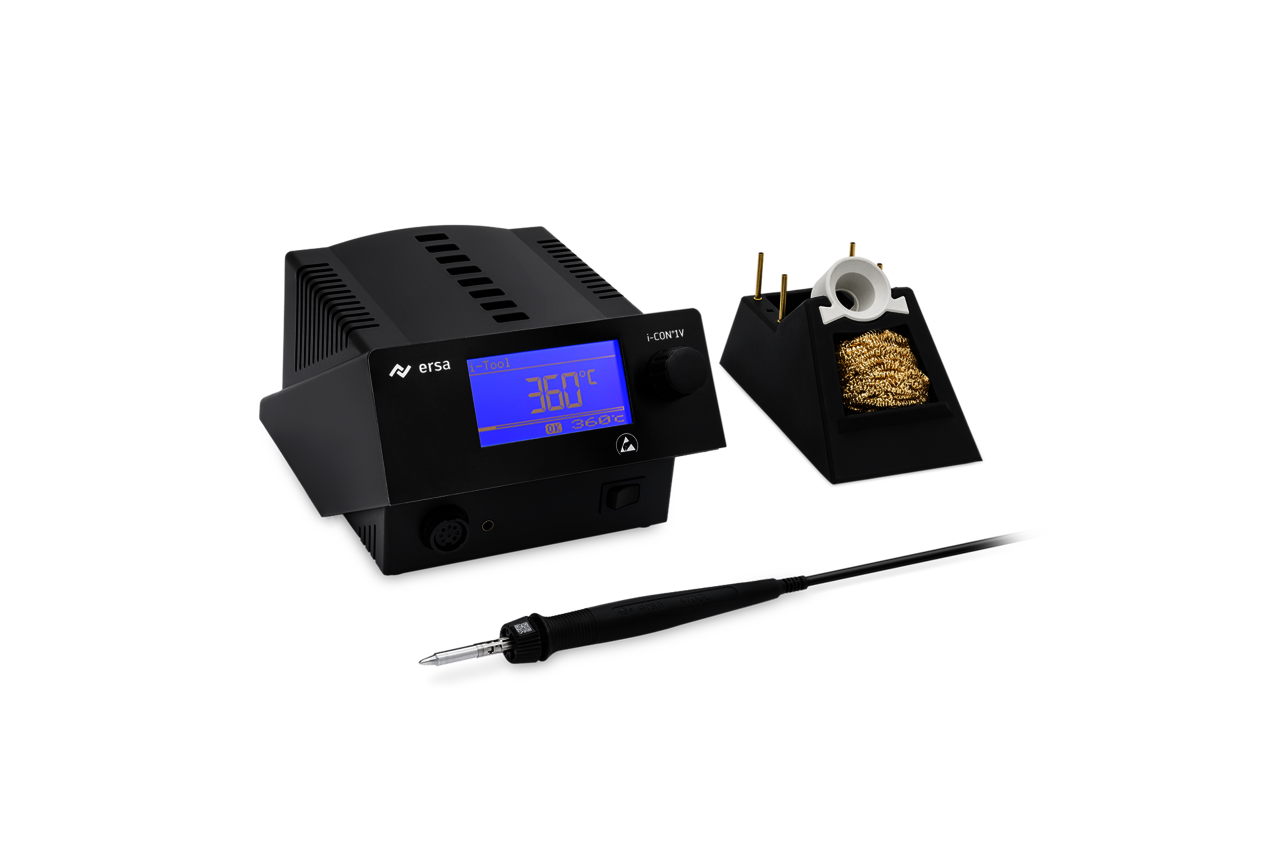
Solderinf station Ersa i-Con 1V
one-channel, electronically controlled soldering and desoldering station, max. 150 W
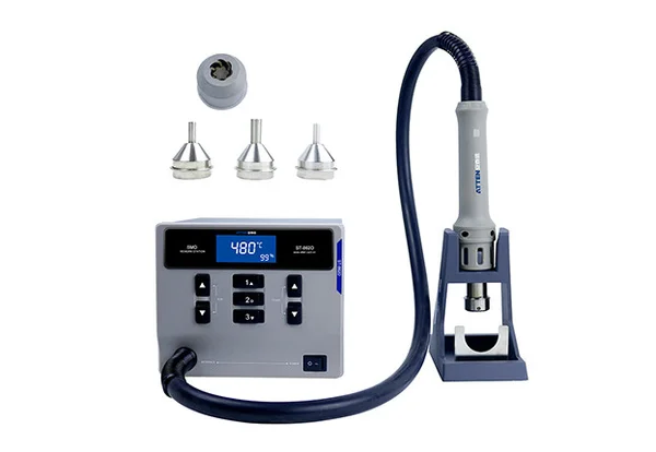
Hot air rework station Atten ST862D
100 to 480 degC, 1000 W
Industrial Microscope Digital Camera
16MP 1080P 60FPS HDMI USB FHD
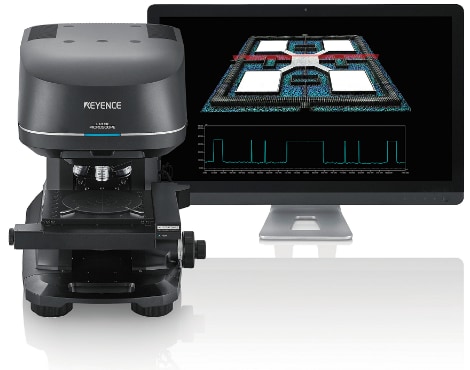
VK-X1000
The Keyence VK-X1000 with VK-X1050 head is a 3D confocal laser scanning microscope for high-resolution hybrid surface inspection and metrology. It combines…
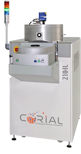
Custom
A Cluster Tool integrates multiple processing chambers, optimizing semiconductor fabrication by combining Si-based PECVD (Plasma Enhanced Chemical Vapor De…
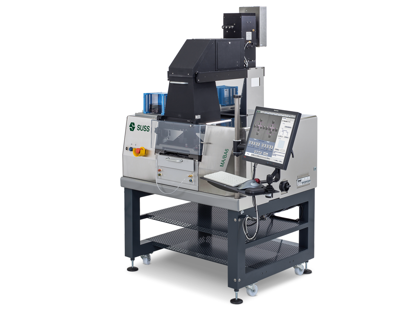
ma6ba6gen4
SUSS MicroTec MA6/BA6 gen4 is an industry-grade UV mask aligner for contact and proximity lithography with backside alignment capability, installed in the …
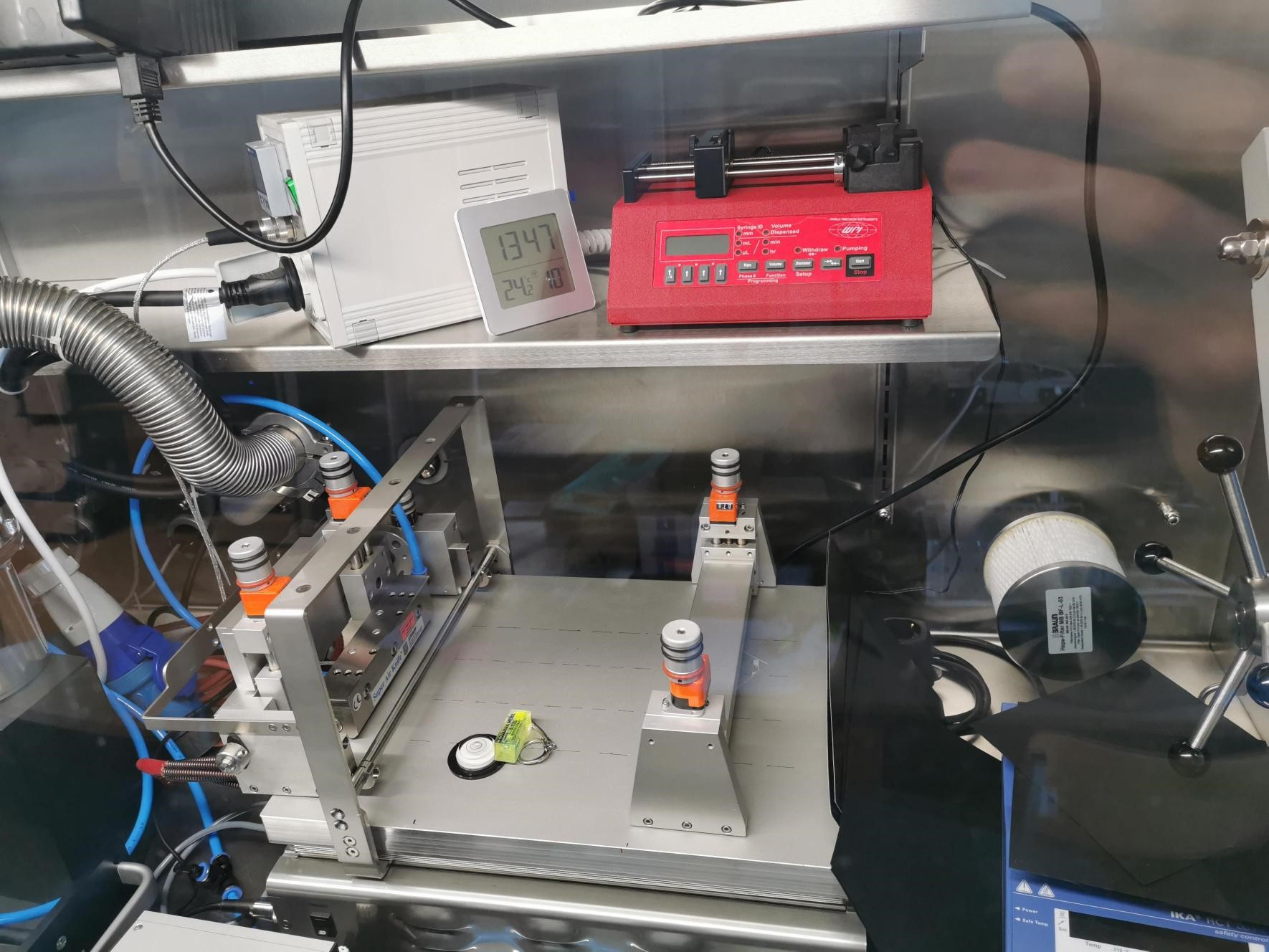
Slot-die and blade coater / Naprava za nanos raztopin s postopkom slot-die in blade coating
The tool handles solution processing using slot-die and blade-coating. It is positioned in a glovebox.
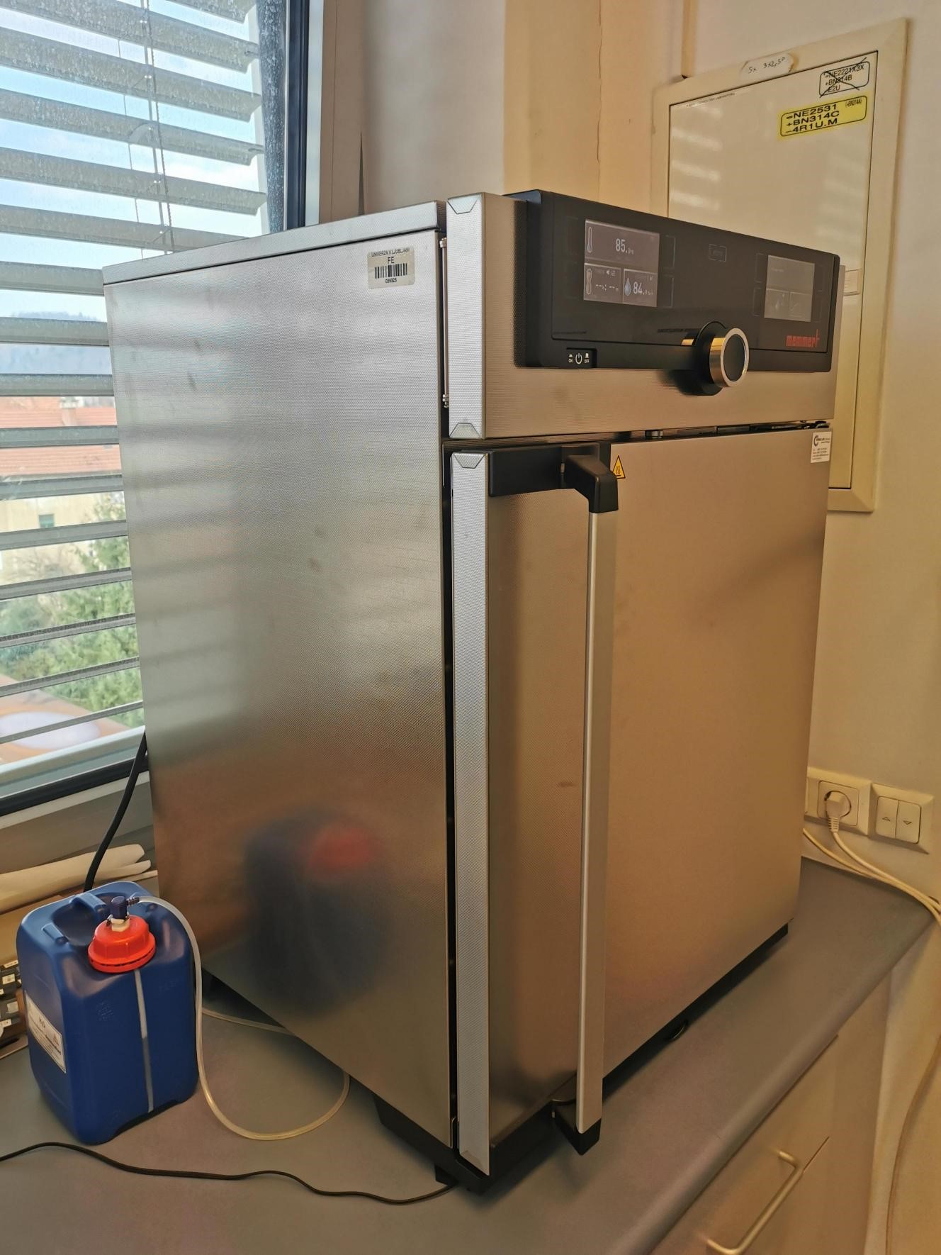
Climate chamber HCP50
Climate humidity chamber HCP50 Temperature range: +18 - +90 °C Rel. humidity range: 20 – 95% Volume: 56 l
Photonic Integrated Circuit Characterisation System
The system is designed for the optical and electrical characterisation of photonic integrated building blocks and various photonic integrated circuits.
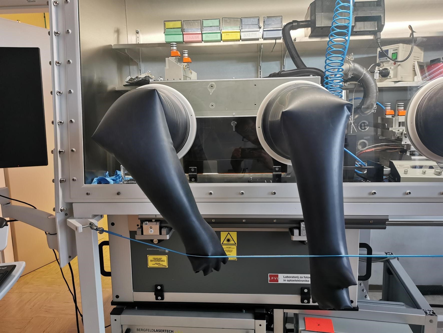
Laser system for the fabrication of thin-film minimodules
he laser system is intended for the microstructuring of thin layers and is primarily used for the fabrication of thin-film (perovskite) minimodules with th…
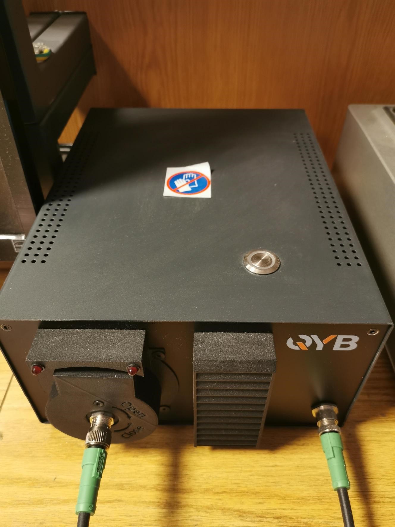
Photoluminescence and Electroluminescence Measurement System LuQY Pro
The system is capable of measuring the photo- and electroluminescence of smaller thin-film samples.
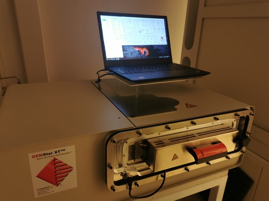
Thin film deposition equipment
Thin film deposition equipment
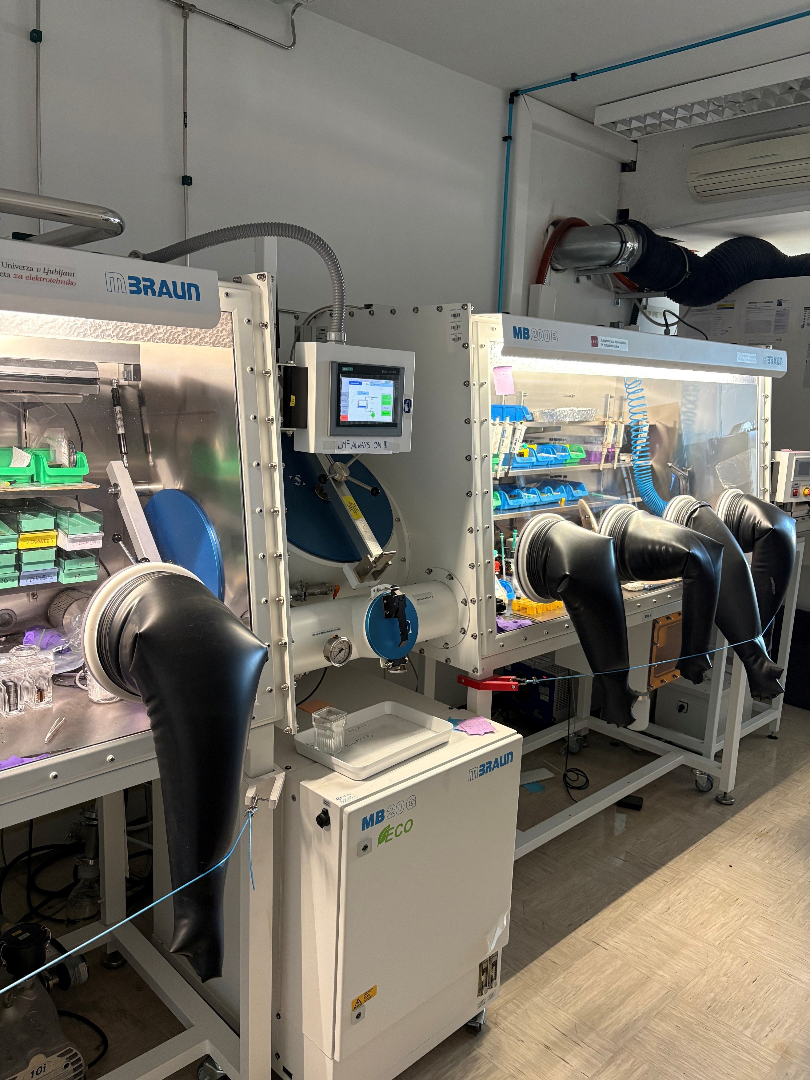
Thin film PV technology set-up
Inertial chamber (N2) for deposition steps without presence of humidity or oxygen) and ink-jet printer for depostion of inorganic or organic inks to layers…
PVS component evaluation set-up
Isolation resistivity test of PV modules, climate chamber testing of PV modules, conversion efficiency measurement of inverters.
Solar Simulator AM1.5
Measurement of conversion efficiency under solar irradiance AM1.5.
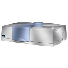
UV/Vis/NIR Spectrophotometer
Measurement of direct and total transmission and reflection in the wavelength range from175 to 3300 nm.
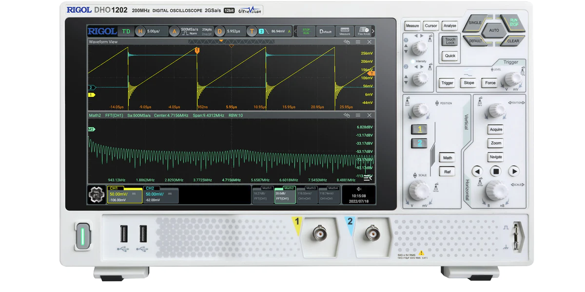
Digital Oscilloscope 200MHz, 12bit, 2GSa/s, 2 CH ( 4x)
https://www.batronix.com/shop/oscilloscopes/Rigol-DHO1202.html
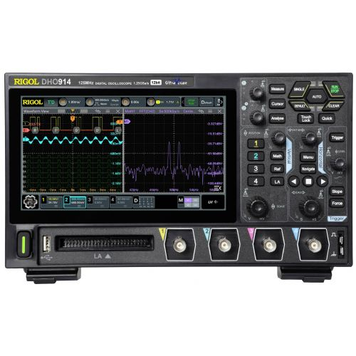
DHO914, 21 pcs
Digital Oscilloscope 125MHz, 1.25GSa/s, 4 channels, 16 digital channels
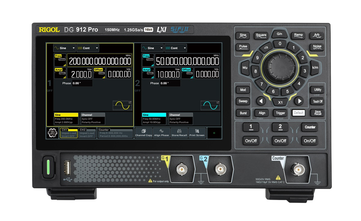
DG912 Pro, 21 pcs
Function/Arbitrary Waveform Generator 150MHz,1.25GSa/s,16bit,2CH
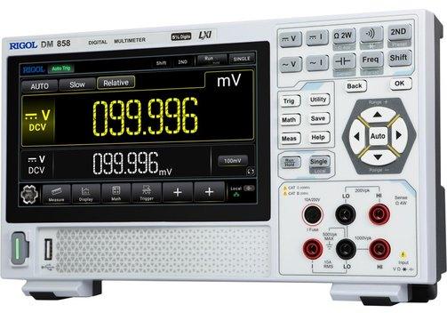
DM858, 21 pcs
Digital Multimeter 5.5 digits Resolution, 125 rdgs/s, 0.03% 1-Year DCV Accuracy
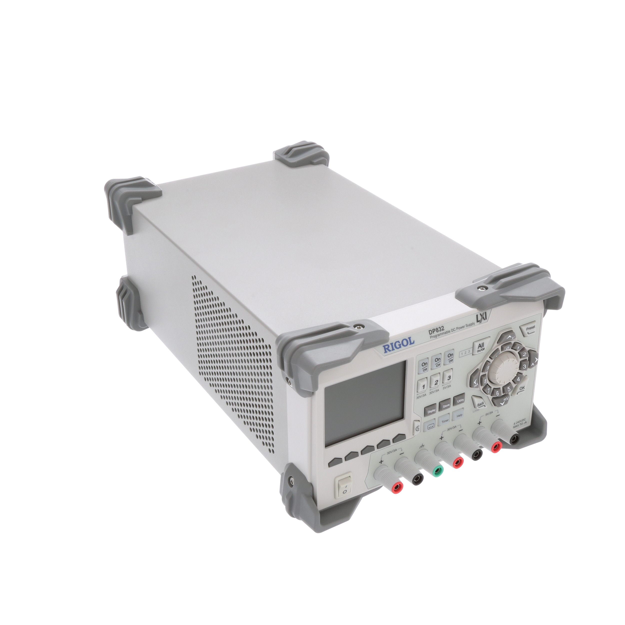
DP832, 21 pcs
Programmable Linear DC Power Supply 195W, 3CH(30V/3A || 30V/3A,5V/3A),10mV/10mA resolution. Ripple<350uV
DHO924S, 10 pcs
250MHz, 1.25GSa/s, 4 channels, 16 digital channels
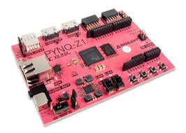
PYNQ-Z1 with Accessory Kit, 10 pcs
The PYNQ-Z1 board is designed to be used with PYNQ, a new open-source framework that enables embedded programmers to exploit the capabilities of Xilinx Zyn…
16 Channel Digital Logic Probe
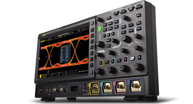
MSO8104
1 GHz, 10 GSa/s, 500 Mpts, 4+16 CH MSO
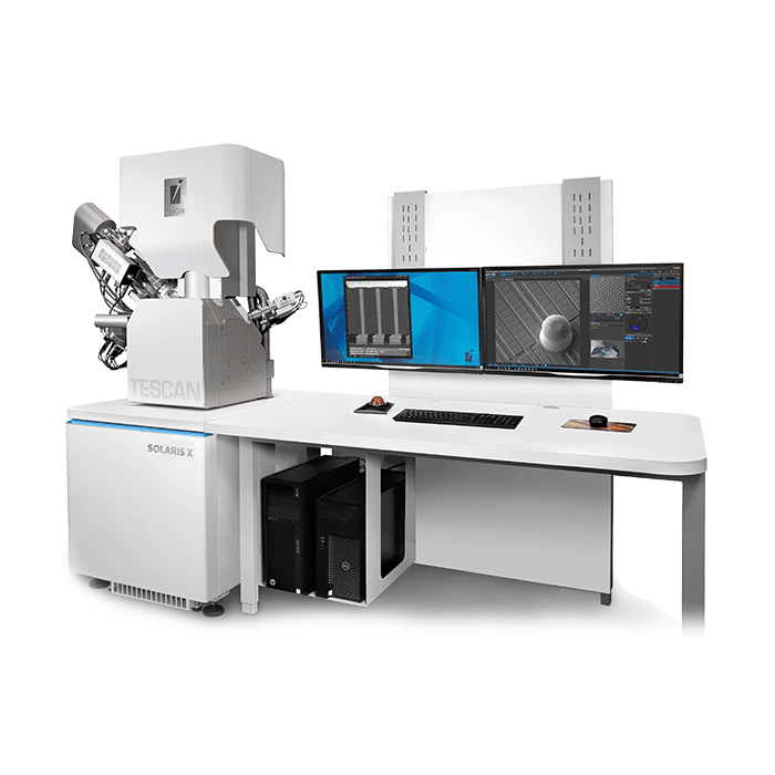
Micro/nano lithographic and machining SEM/FIB system / Mikro/nano obdelovalni in litografski sistem s SEM/FIB
R&D platform Solaris for direct micromachining (FIB milling and FIB-assisted deposition), electron beam lithography, ion-beam lithography and sample observ…
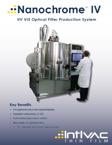
Thin film deposition system / Sistem za depozicijo tankih plasti
A thin film deposition system NanoChrome IV is capable of producing high quality dielectric thin film layers
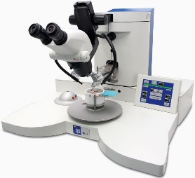
Die Bonder / Sistem za leplenje polprevodniških naprav
Semi automatic R&D die bonding system for microelectronics
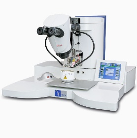
Wire bonder/ Sistem za žično povezovanje polprevodniških naprav
Semi automatic R&D wire bonding system for microelectronics
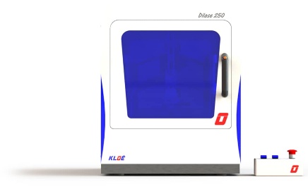
Laser lithography system / Sistem za lasersko litografijo
The maskless equipment Dilase 250 is a versatile and compact equipment, which gives access to laser lithography.
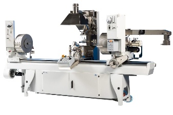
MCVD preform fabrication system / MCVD sistem za izdelavo vlakenskih surovcev
MCVD system for fabrication of custom specialty (doped) optical fibers.
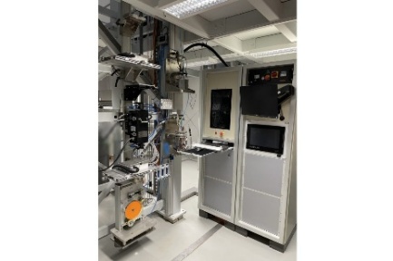
Drawing Tower/ Vlečni stolp
Optical fiber drawing tower equipped with versatile system for applying special fiber coatings and advanced monitoring systems, allowing of fabrication of …
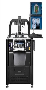
300 mm semi-/ fully-automated probe system
Modular 300 mm wafer probe station used for on-wafer electrical characterization (DC, RF, I-V/C-V, noise etc.) in device research and development. It suppo…
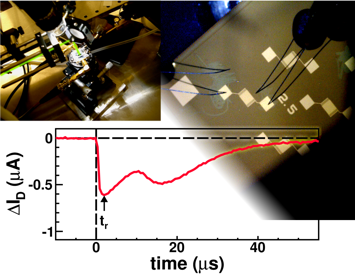
Time-of-Flight Photoconductivity
Time-of-flight photoconductivity is an experimental method to measure charge carrier mobility in semiconducting and insulating materials.
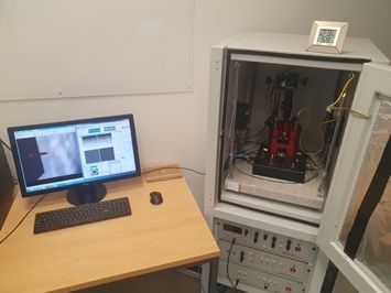
Atomic Force Microscope (AFM) with conductive and kelvin mode probes
This equipment combines high-resolution surface imaging with detailed electrical and work function measurements, offering versatile analysis for a wide ran…
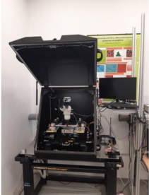
Current-voltage measurement with Four-Probe Station
With the four-probe station, we can measure various electrical properties of materials, including: - Resistance - Sheet Resistance - Conductivity - Curren…
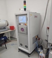
Plasma cleaning chamber
Plasma chamber for surface cleaning, sterilization, surface activation and improvement of material properties.
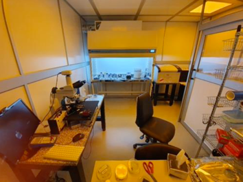
Clean room with laser lithography
Clean room enables a dust-free environment. Monmouth Scientific, CAM2250 filter, dimensions 3.5m x 3.5m, internal height 2.4m, yellow light.
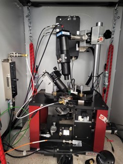
Scanning Near-Field Microscope SNOM
Scanning Near Field Optical Microscopy (SNOM) is an advanced imaging technique that breaks the diffraction limit of conventional optical microscopy. By usi…
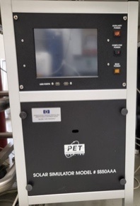
Solar cells characterization setup
The solar simulator is a sophisticated light source that approximates natural sunlight using a high-pressure xenon lamp.
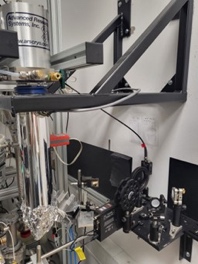
Closed-cycle He-cooled cryostat with quartz window and GHz feed-through connection (10-300K)
To test electrooptical properties of material as a function of temperature, the testing material should be cooled with cryostat. Cryostat is a device used …
Alignment system for 2D materials
The system allows precise (~1µm) positioning and stacking of 2D materials.
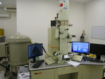
Transmission Electron Microscope (TEM) with STEM and EDX unit
It is possible to examine the solid specimens with atomic resolution (nominal resolution 0.1 nm).
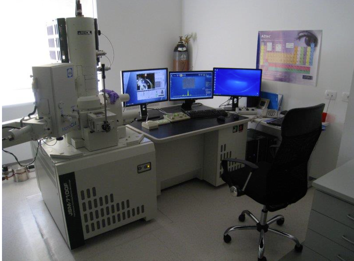
Scanning Electron Microscope (SEM), with backscattered detector, EDX unit, cathodoluminescence and heating stage
With the microscope it is possible to examine the surface of solid specimens with nanometric resolution (typical resolution 3 nm)
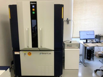
Advanced X-ray diffractometer
With this X-ray diffractometer, we can determine the phase composition of powdered materials.
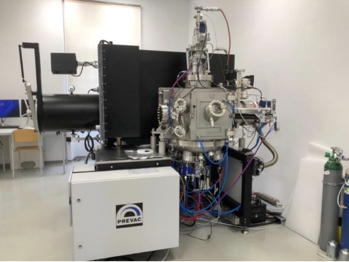
System for thin films deposition and physical vapor deposition (PVD)
The deposition system, allows to grow thin films of magnetic materials oxides and dielectrics for applications in devices. The system includes: - Glovebo…
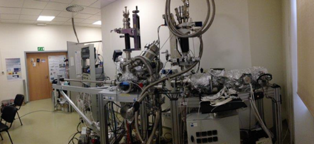
Experimental set up for photoemission spectroscopy
Performing XPS (X ray photoemission spectroscopy) and UPS (ultraviolet photoemission spectroscopy) measurements in the conventional and also in the time re…